报告一:Electron Ptychography
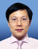
主讲嘉宾:Prof. Peng Wang(Nanjing University)
时间: 7月26日(周四)9:00-10:30
报告二:锂电池层状正极材料衰退机理的电子显微学研究
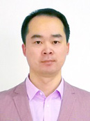
主讲嘉宾:闫鹏飞 教授(北京工业大学 固体所)
时间: 7月26日(周四)10:30-12:00
地点:李薰楼468会议室
报告一简介:
Transmission electron microscopy (TEM) is a powerful tool for material science characterization due to its high spatial resolution. Coherent diffraction imaging (CDI) [1] is a "lensless" method that forms an image of an object by solving the phase problem from a single diffraction pattern with an iterative phasing algorithm. This approach can, in principle, overcome the current image resolution limiting factors and ultimately achieve wavelength-limited resolution. However, conventional CDI experiments require isolated samples and a priori knowledge about the sample shape or extent. Maiden and Rodenburg suggested an extended ptychographical iterative engine (ePIE), which does not need this prior information and overcomes many of the other issues of CDI, such as convergence stagnation and limited field of view. Recently, two-dimensional (2D) ptychographical reconstructions at atomic lateral resolution [2] have been achieved using ePIE [3] on a CeO2 nanoparticle. However, when the sample becomes thicker, the multiplicative assumption of electron-sample interaction becomes invalid causing the ptychographical reconstruction to breakdown. To overcome this limitation, Maiden et al. incorporated the well-known multiple slice solution to multiple scattering into the ePIE algorithm (3PIE) [4]. In this approach the sample is split into axial sections, to produce 3D optically sectioned images of the sample. This 3D multiple-section reconstruction of ptychography has been successfully demonstrated with both light [4] and X-ray [5] optics recently. However, this method is still a challenge for use with the electrons. In this paper, we will firstly review our previous work on the capabilities of defocused probe ptychography to achieve a 2D phase reconstruction of a nanocrystal at sub-? resolution [6] and a 3D reconstruction of nanostructured materials [7] using traditional CCD camera. Subsequently we will show results from focused and defocused electron ptychography using a fast direct electron detector to reconstruct the wavefunction of various low dimensional materials under different low dose conditions.
References
[1]R Gerchberg and WO Saxton, Optik 35 (1972), p. 237-246.?
[2]AJ D’Alfonso, AJ Morgan, AW Yan, et al., Physical Review B 89 (2014), p. 064101.
[3]AM Maiden and JM Rodenburg, Ultramicroscopy 109 (2009), p. 1256-1262.?
[4]AM Maiden, MJ Humphry and JM Rodenburg, Journal of the Optical Society of America a-Optics Image Science and Vision 29 (2012), p. 1606-1614.
[5]A Suzuki, S Furutaku and K Shimomura, et al., Physical Review Letters 112 (2014), p. 053903.?
[6] P Wang, et al., Scientific Reports 7 (2017) , p.2857.
[7] S Gao, et al., Nature Communications, 8 (2017), p.163.
主讲嘉宾一简介:
 Professor Peng Wang received his Ph.D degree in Engineering from University of Liverpool, UK in 2006. He was a research associate at SuperSTEM Laboratory in UK from 2007 to 2008. From 2008 to 2012 he worked as a research fellow in electron microscopy group at Oxford University. He joined Nanjing University (NJU), China as a Professor in 2012 and setup Nanjing Sub-atomic Resolution EM Laboratory in NJU. Prof. Wang's research interests have been in the applications of aberration corrected scanning transmission electron microscopy (STEM) imaging and electron energy loss spectroscopy to characterize materials at nano and atomic scales from two to three dimensions. He had developed a technique of 3D imaging materials at the nano-scale using scanning confocal electron microscopy (SCEM) performed on a double aberration-corrected TEM. Running confocal configuration on high-resolution TEM can improve depth of field to the atomic level so that the characterizations are spatially well-defined at selected depth. Currently his work is focused on developing an advance Coherent Diffractive Imaging technique, so called Ptychography. In last 5 years, the applicant has published 61 peer-reviewed papers in journals, which contains 21 first or corresponding authored paper including Nature Electronic, Nature Communications and Advanced Functional Materials. Professor Wang is a member of Institute of Physics (MInstP), Youth Committee of Chinese Materials Research Society (CMRS), Committee of Chinese Electron Microscopy Society and Committee of Chinese Crystallography Society. His research had been supported by “the Thousand Talents Plan” Program for Distinguished Young Scholars from 2012-2015.
Contact information:
National Laboratory of Solid State Microstructures, College of Engineering and Applied Sciences and Collaborative Innovation Center of Advanced Microstructures, Nanjing University, Nanjing 210093, People’s Republic of China.
wangpeng@nju.edu.cn
Selected Recent Publications:
1. Wang, M, et al. Nature Electronics, 1, 130-136 (2018).
2. Huang, Q., et al. Nano Energy, 44, 336-344 (2018).
3. Gao, S., et al. Nature Communications, 8, 163 (2017).
4. Wang, P., et al. Scientific Reports, 7, 2857 (2017).
5. Zhong, Y., et al. Advanced Functional Materials, 26, 7156–7163 (2016).
6. Zhao, Y., et al,. Advanced Functional Materials, 26, 4760–4767 (2016).
报告二简介:
透射电子显微学在最近的十几年中得到了突飞猛进的发展,主要表现为两个方面:一是分辨率的不断提升; 包括空间分辨本领,能量分辨本领和时间分辨本领。另一方面,原位电镜技术的发展更是日新月异;使得材料发生物理化学变化的动态过程可以直接进行观测。这些技术的发展为材料和化学科研人员提供了更丰富多样的手段去探究材料构效和演变的基本科学规律。在本报告中,闫鹏飞博士将主要介绍透射电镜在储能材料中的应用,尤其是层状氧化物正极材料的失效机制和调控机制。展示透射电镜在原子分辨率成像,元素成像,元素价态分析上的应用,以及原位技术的应用。
主讲嘉宾二简介:
 闫鹏飞博士, 于2004年本科毕业于中南大学材料科学与工程学院, 于2010年博士毕业于中国科学院金属研究所固体原子像研究部,从事透射电镜方面的学习和研究。2010~2013年在日本NIMS从事固体氧化物燃料电池的相关研究。2013~2017年在美国太平洋西北国家实验室(PNNL)从事锂电池方面的透射电镜研究。 2017年10月入职北京工业大学固体微结构与性能研究所,校聘教授,北京市青年海聚人才。 目前,主要研究方向是储能材料的电子显微学分析. 已经发表的第一作者文章19篇,包括Nature Materials,Nature Energy,Nature Communications (2), Advanced Materials, Advanced Energy Materials, Nano Letters (3), Chemistry of Materials (4)等。另外,合作发表SCI文章60余篇。2015年,美国显微分析学会授予“Presidential Scholar Award”。 2016年所在太平洋西北国家实验室授予“Pathway to Excellence Award”。担任Nature Communications, Advanced Energy Materials, Nano Letters, Nano Energy等国际知名期刊的审稿人。

