教育和工作经历
2021.11-至今, 中国科学院金属研究所,研究员。
2019.5-2020.6, 美国加州大学洛杉矶分校,访问学者。
2012.10-2021.11,中国科学院金属研究所,副研究员。
2009.7-2012.10, 中国科学院金属研究所,助理研究员。
2005.9-2009.6, 中国科学院金属研究所,工学博士。
石墨烯的CVD制备与柔性光/电器件应用。
沈阳市拔尖人才;SYNL青年创新奖
[1] L. P. Ma#, S. C. Dong#, H. M. Cheng, W. C. Ren*, Breaking the rate-integrity dilemma in large-area bubbling transfer of graphene by strain engineering. Adv. Funct. Mater. 2021, 2104228.
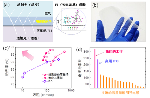
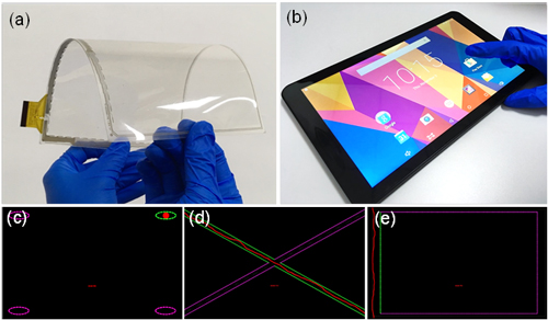
[2] L. P. Ma, Z. B. Wu, L. C. Yin, D. D. Zhang, S. C. Dong, Q. Zhang, M. L. Chen, W. Ma, Z. B. Zhang, J. H. Du, D. M. Sun, K. H. Liu, X. F. Duan, D. G. Ma, H. M. Cheng, W. C. Ren*, Pushing the conductance and transparency limit of monolayer graphene electrodes for flexible organic light-emitting diodes. Proc. Natl. Acad. Sci. U.S.A. 2020, 117, 25991.
[3] T. Aziz#, S. J. Wei#, Y. Sun, L. P. Ma*, S. F. Pei, S. C. Dong, W. C. Ren, Q. Liu, H. M. Cheng, D. M. Sun*, High-performance flexible resistive random access memory devices based on graphene oxidized with a perpendicular oxidation gradient. Nanoscale 2021, 13, 2448.
[4] S. J. Wei, Y. B. Hao, Z. Ying, C. Xu, Q. W. Wei, S. Xue, H. M. Cheng, W. C. Ren, L. P. Ma*, Y. Zeng*, Transfer-free CVD graphene for highly sensitive glucose sensors. J Mater Sci Technol 2020, 37, 71.
[5] M. Guo, L. P. Ma, W. C. Ren, T. S. Lai*, Control of the ultrafast photo-electronic dynamics of a chemical-vapor-deposited-grown graphene by ozone oxidation. Photonics Res 2020, 8, 17.
[6] S. J. Wei#, L. P. Ma#, M. L. Chen, Z. B. Liu, W. Ma, D. M. Sun, H. M. Cheng*, W. C. Ren*, Water-assisted rapid growth of monolayer graphene films on SiO2/Si substrates. Carbon 2019, 148, 241.
[7] D. D. Zhang#, J. H. Du#, Y. L. Hong, W. M. Zhang, X. Wang, H. Jin, P. L. Burn, J. S. Yu, M. L. Chen, D. M. Sun, M. Li, L. Q. Liu, L. P. Ma, H. M. Cheng, W. C. Ren*, A double support layer for facile clean transfer of two-dimensional materials for high-performance electronic and optoelectronic devices. ACS Nano 2019, 13, 5513.
[8] L. P. Ma, W. C. Ren*, H. M. Cheng, Transfer methods of graphene from metal substrates: a review (Invited review). Small Methods 2019, 3, 13.
[9] L. P. Ma#, S. C. Dong#, M. L. Chen, W. Ma, D. M. Sun, Y. Gao, T. Ma, H. M. Cheng, W. C. Ren*, UV-epoxy-enabled simultaneous intact transfer and highly efficient doping for roll-to-roll production of high-performance graphene films. ACS Appl. Mater. Interfaces 2018, 10, 40756.
[10] Z. K. Zhang#, J. H. Du#, D. D. Zhang, H. D. Sun, L. C. Yin, L. P. Ma, J. S. Chen, D. G. Ma, H. M. Cheng, W. C. Ren*, Rosin-enabled ultraclean and damage-free transfer of graphene for large-area flexible organic light-emitting diodes. Nat. Commun. 2017, 8, 9.
[11] X. Gan, R. T. Lv, H. Y. Zhu, L. P. Ma, X. Y. Wang, Z. X. Zhang, Z. H. Huang, H. W. Zhu, W. C. Ren, M. Terrones, F. Y. Kang*, Polymer-coated graphene films as anti-reflective transparent electrodes for Schottky junction solar cells. J. Mater. Chem. A 2016, 4, 13795.
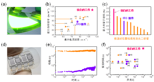
[12] S. Jia, H. D. Sun, J. H. Du, Z. K. Zhang, D. D. Zhang, L. P. Ma, J. S. Chen, D. G. Ma, H. M. Cheng, W. C. Ren*, Graphene oxide/graphene vertical heterostructure electrodes for highly efficient and flexible organic light emitting diodes. Nanoscale 2016, 8, 10714.
[13] Y. Gao, Z. B. Liu, D. M. Sun, L. Huang, L. P. Ma, L. C. Yin, T. Ma, Z. Y. Zhang, X. L. Ma, L. M. Peng, H. M. Cheng, W. C. Ren*, Large-area synthesis of high-quality and uniform monolayer WS2 on reusable Au foils. Nat. Commun. 2015, 6, 10.
[14] J. H. Du, S. F. Pei, L. P. Ma, H. M. Cheng*, Carbon nanotube- and graphene- based transparent conductive films for optoelectronic devices. Adv. Mater. 2014, 26, 1958.
[15] J. T. Yuan#, L. P. Ma#, S. F. Pei, J. H. Du, Y. Su, W. C. Ren, H. M. Cheng*, Tuning the electrical and optical properties of graphene by ozone treatment for patterning monolithic transparent electrodes. ACS Nano 2013, 7, 4233.
近期国际国内会议报告及任职等:
[1] L. P. Ma, W. C. Ren, H. M. Cheng, Simultaneous Improvement in Conductance and Transparency of Flexible Graphene Transparent Electrode by Antireflective Dopant, 2021 International Forum on Graphene in Shenzhen, Shenzhen, 8-11 April, 2021. Invited presentation.
[2] L. P. Ma, W. C. Ren, H. M. Cheng, Epoxy-Enabled Simultaneous Intact transfer and Highly Efficient Doping for Roll-to-Roll Production of High-Performance Graphene Films, Graphene 2018, Dresden (Germany), 26-29 June, 2018. Oral presentation.
[3] L. P. Ma, W. C. Ren, H. M. Cheng, A Versatile p-type Dopant for High-performance Flexible Graphene Transparent Electrode and its Application in Optoelectronic Devices, RPGR 2017 (the 9th annual Recent Progress in Graphene and Two-dimensional Materials Research Conference), Singapore, 19-22 September, 2017. Oral presentation.
[4] L. P. Ma, W. C. Ren, H. M. Cheng, High-performance Graphene-based Transparent Conductive Films Fabricated by Roll-to-roll Processes, RPGR 2016 (the 8th International Conference on Recent Progress in Graphene-2D Research), Seoul (Korea), 25-29 September, 2016. Oral presentation.
[5] 马来鹏,石墨烯的CVD低成本制备及其在柔性触屏和有机发光二极管中的应用, 石墨烯在触屏,可穿戴电子产品应用投资高峰论坛, 上海, 2015年7月8日。邀请报告。
[6] L. P. Ma, W. C. Ren, H. M. Cheng, Tuning the Electrical and Optical Properties of Graphene by Ozone Treatment for Patterning Monolithic Transparent Electrodes, RPGR 2013 (Recent Progress in Graphene Research 2013), Tokyo (Japan), 9-13 September, 2013. Oral presentation.
授权发明专利:
[1] 任文才,高力波,马来鹏,成会明,一种低成本无损转移石墨烯的方法,授权公告日:2014.09.03,中国专利号:ZL 201110154465.9
[2] 任文才,高力波,马来鹏,成会明,一种低成本无损转移石墨烯的方法,授权公告日:2015.12.22,美国专利号: US 9,216,559 B2
[3] 任文才,高力波,马来鹏,成会明,一种低成本无损转移石墨烯的方法,授权公告日:2016.03.16,欧盟专利号:EP 2719797 B1
[4] 任文才,高力波,马来鹏,成会明,一种低成本无损转移石墨烯的方法,授权公告日:2015.11.20,日本专利号:5840772
[5] 任文才,高力波,马来鹏,成会明,一种低成本无损转移石墨烯的方法,授权公告日:2015.06.09,韩国专利号:10-1529012
[6] 任文才,高力波,马腾,高旸,马来鹏,成会明,一种大尺寸单晶石墨烯及其连续薄膜的制备方法,授权公告日:2014.11.05, 专利号:ZL 201210024680.1
[7] 杜金红,袁江潭,苏阳,马来鹏,裴松峰,成会明,一种臭氧调控纳米碳质薄膜光电性能及图案化的方法,授权公告日:2014.06.11,专利号:ZL 201310156354.0
[8] 杜金红,苏阳,马来鹏,裴松峰,刘文彬,刘畅,成会明,一种无损,无污染的纳米碳质薄膜的图案化方法,授权公告日:2015.08.12,专利号:ZL 201110187013.0
[9] 任文才,马来鹏,成会明,一种低成本,洁净无损转移大面积石墨烯的方法,授权公告日:2017年2月15日,专利号:ZL 201410376865.8
[10] 任文才,马来鹏,成会明,一种稳定掺杂的大面积石墨烯透明导电膜规模化制备方法,授权公告日:2017年2月22日,专利号:ZL 201410709308.3
[11] 任文才,马来鹏,成会明,一种通过调控结合力转移大面积石墨烯的方法,授权公告日:2017年1月11日,专利号:ZL 201410709278.6
[12] 任文才,马来鹏,成会明,一种CVD生长大面积石墨烯的规模化方法,授权公告日:2018年1月16日,专利号:ZL 201510039352.2
[13] 任文才,马来鹏,成会明,一种低成本生长大面积石墨烯的CVD方法,授权公告日:2018年3月9日,专利号:ZL 201510039341.4
[14] 任文才,马来鹏,成会明,一种卷对卷连续转移石墨烯的装置,授权公告日:2019年2月19日,专利号:ZL 201510237119.5
[15] 任文才,马来鹏,成会明,一种无损转移大面积石墨烯的方法,授权公告日:2019年6月7日,专利号:ZL 201510645447.9
[16] 杜金红,张志坤,张鼎冬,马来鹏,任文才,成会明,一种松香树脂转移石墨烯的方法及石墨烯透明导电薄膜的制备与应用,授权公告日:2019年8月16日,专利号:ZL 201611065371.3
[17] 马来鹏,任文才,董世超,成会明,一种稳定掺杂石墨烯的化学掺杂剂与掺杂方法,授权公告日:2020年7月10日,专利号:ZL 201610673816.X
[18] 马来鹏,任文才,成会明,采用液相界面层洁净,无损转移大面积二维材料的方法,授权公告日:2021年3月26日,专利号:ZL 201711167326.3
[19] 马来鹏,任文才,董世超,成会明,一种高效掺杂石墨烯的超强酸掺杂剂和掺杂方法,授权公告日:2021年3月26日,专利号:ZL 201610854519.5
授权实用新型专利:
[1] 凌桦光,孟磊,马来鹏,任文才,成会明,石墨烯电容屏的层状结构,授权公告日:2015年1月7日,专利号:ZL 201410295202.3
[2] 凌桦光,孟磊,马来鹏,任文才,成会明,一种石墨烯电容式触摸屏的层状结构,授权公告日:2015年1月7日,专利号:ZL 201410294608.X
 官方公众号
官方公众号